Electronics tech notes, part 6: designing a power protection board for onboard computing
Executive summary
During the past week I designed a power protection board for integrating an onboard computer into a drone.
The next version of my custom drone requires an onboard computer integrated into the rest of the electronics. Different subsystems that were not designed to work together by the manufacturer need an additional protection stage. This custom PCB solves exactly that problem.
It is not a sophisticated board, but it is my first experience of designing a PCB to close the gap between project requirements and what the market currently offers. That is why the full production chain and technological process described here may be of interest to potential clients.
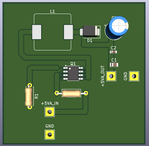
The problem
The second version of my custom drone needs a video stream from the air and the ability to perform custom processing on board. An onboard computer is required for this. An upgrade to a 21–38 TOPS class computer is planned later to support fully autonomous navigation.
The chosen computer is designed to work with its official power adapter. It can also be powered through GPIO pins from an external source, but connecting the battery directly requires proper voltage and current matching as well as protection against several threats. The official adapter already provides these functions. Therefore I needed to implement an equivalent solution that would allow the computer to be powered safely from the drone’s battery.
Market research identified a suitable DC-DC converter (К480508) that supports a wide input voltage range covering all common battery types and delivers a stable 5 V output at up to 8 A.
What the market lacks is a compact protection circuit that guards the computer against voltage transients, reverse polarity, backfeeding and short circuits. This is the reason a custom PCB was required.
The solution
Design of the principle schematic
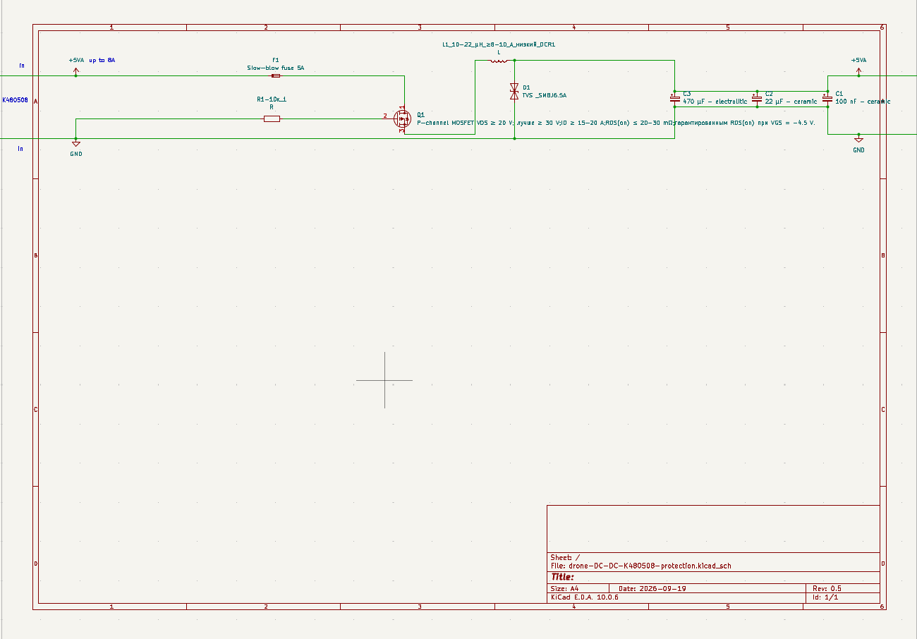
The board has a 5 V / 5 A input and a 5 V / 5 A output. Although the selected DC-DC converter can provide up to 8 A, the protection board is designed for a 5 A continuous load. Between the input and output, a fuse protects against overcurrent, while a MOSFET is used as a low-loss reverse-polarity and reverse-current protection element.
A conventional diode was rejected because of its forward voltage drop. At 5 V this drop becomes significant. A MOSFET with a gate resistor provides a much lower voltage drop while still blocking reverse current. The fuse on the source side protects the circuit from overcurrent. With the MOSFET oriented as shown, its body diode blocks reverse current when the input supply is absent, preventing backfeeding from the output.
The MOSFET was selected not only for its current rating but also for its low RDS(on) at the available gate-source voltage.
In addition, the switching elements and the dynamic nature of the drone introduce noise that must be filtered. An LC filter consisting of a series inductor and several capacitors of different values is used to reduce switching noise over a broad frequency range. It is important to keep the physical distance between the inductor, the capacitors and the output as short as possible.
PCB design
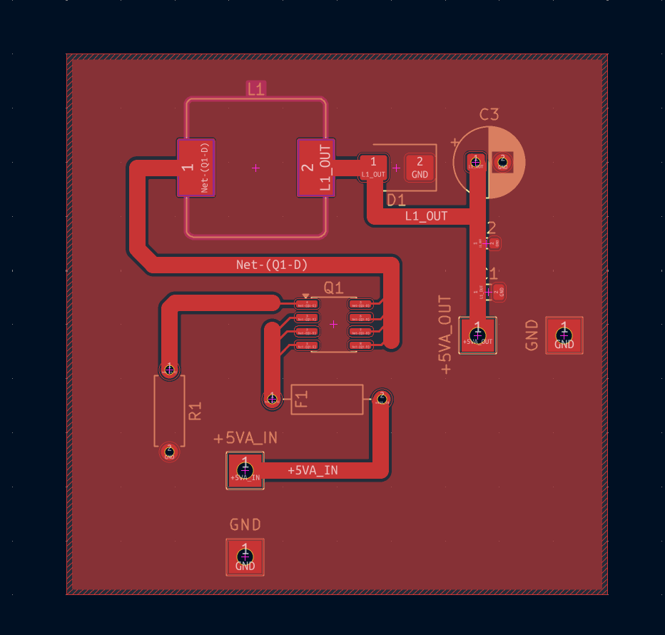
Both the schematic and the PCB were designed in KiCad. The software can automatically transfer the schematic to the board layout, but the result is rarely perfect and several manual steps are required.
The first step is choosing the correct footprints. Every component has its own package and pin configuration, so selecting the right footprint from the library is critical.
The next challenge is routing. Two common problems appeared during this stage.
The first is incorrect footprint pin mapping. If the wrong footprint is assigned, the pins end up in the wrong physical positions and the connections become invalid.
The second is “phantom” connections. A visual connection may look correct, yet the software can still report that the nets are not connected. This is important because the manufacturing data is generated from the internal netlist, not from the visual appearance of the board. The solution was to check the actual net assignments rather than relying on the visual representation alone.
Current-carrying tracks also require special attention. 5 A is a relatively high current and requires significantly wider copper than the usual 0.2 mm signal tracks; in this design the main power paths were approximately 1.5 mm wide. The MOSFET pins are too close together to accept such wide tracks directly. The workaround is to keep short narrow tracks from the pins and then immediately expand them into the required wide copper.
A large ground plane was used to provide low-impedance return paths and help with EMI. KiCad can create this copper pour automatically while maintaining the required clearance from components and other nets.
Export to Gerber for manufacturing
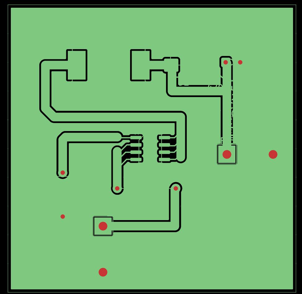
The manufacturer requested Gerber files — the standard format used for PCB fabrication. KiCad can generate them; the main decision is which layers and manufacturing information to include in the final archive.
Manufacturer search and ordering
Several local and China-based PCB manufacturers were evaluated. During negotiations it became clear that the schematic had to be converted into a proper PCB layout and exported as Gerber files. It also turned out that the manufacturer’s CAM software had compatibility issues with Gerber X2, which KiCad can generate by default. Exporting the files without X2 attributes solved the problem. This is a useful detail to remember when dealing with fabrication houses.
Expected result
The project has been sent to the manufacturer for a quotation and production schedule. Once the best offer is selected, the boards will be produced. They will then be tested with a laboratory power supply to verify the design under load and later installed on the drone for final in-flight validation.
Related publications
Electronics tech notes, part I: getting started
Electronics tech notes, part V: assembly of automation for pressure gauge and handmade replacement of the touch panel
Broad vs Narrow specialisation